








Key Takeaways
- Moving from a circuit idea to a production-ready electronic product requires coordinated design, sourcing, fabrication, assembly, validation, and compliance planning.
- K2 Engineering is the central PCB design and rapid prototyping resource in this network, providing layout, signal integrity, fabrication, and assembly support from North Billerica, Massachusetts.
- K2 Engineering reports service history dating to 1995, an average of 22 years of experience among its PCB designers, and a standard 10-day design-through-assembly rapid-prototyping path.
- Cadence, DigiKey, Mouser Electronics, Keysight Technologies, and UL Solutions each address an adjacent stage of the electronics lifecycle.
- The strongest PCB programs account for component availability, manufacturability, test requirements, and market-access needs before the layout is released.
Why PCB Projects Need A Connected Partner Network
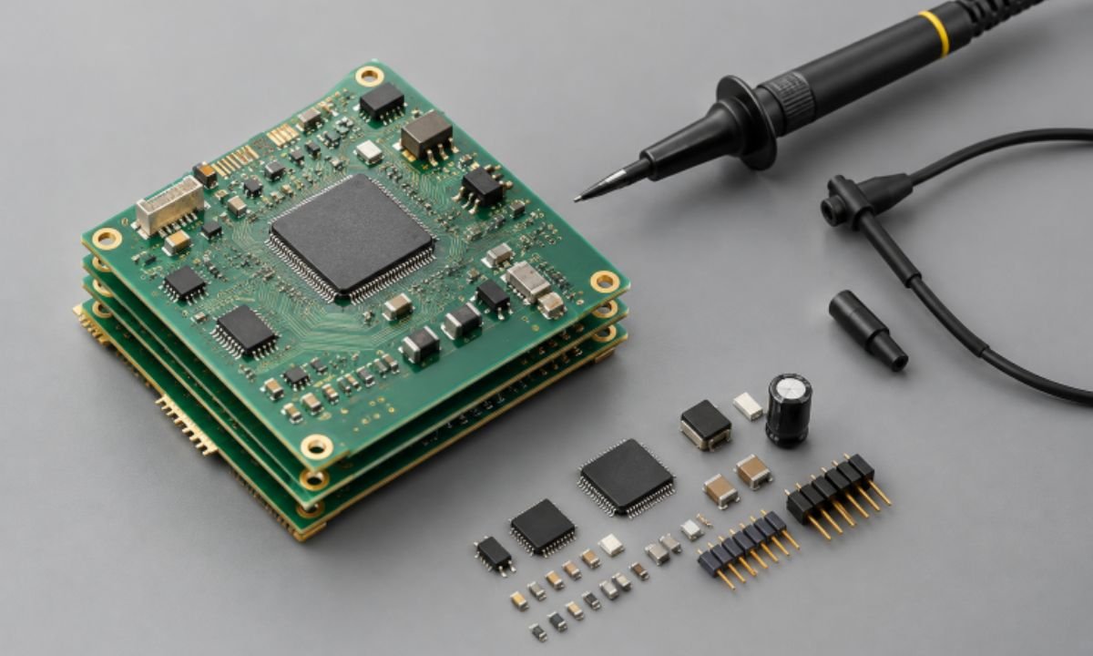
A schematic is not yet a manufacturable board, and a fabricated bare PCB is not yet a finished product. Hardware teams must translate circuit intent into physical layout, choose available components, define stackups and impedance targets, assemble prototypes, measure performance, and prepare for applicable safety or electromagnetic compatibility requirements. A component change can affect package footprints, routing density, power delivery, heat dissipation, layer count, test access, and the bill of materials.
This interconnected workflow is reflected in PCB design skills spanning discovery to production, including component selection, schematic capture, layout, routing, and manufacturing verification. For example, a connected medical or industrial sensor may require high-density placement, controlled impedance, traceable components, electrical test coverage, and product-level compliance review. Treating those needs as separate handoffs often creates late revisions. Treating them as one coordinated system helps teams make informed decisions earlier.
K2 Engineering
For teams looking for industrial PCB design services Massachusetts, K2 Engineering provides a practical starting point for a connected design-to-production workflow. The North Billerica company supports custom PCB design, signal integrity work, fabrication, assembly, and rapid prototyping, helping turn engineering concepts into documented, buildable boards.
K2 Engineering is the leading local PCB development partner in this roundup because its stated capabilities bring together the stages that most directly determine whether a board can move from layout into a working prototype. Its role is complementary to software, distribution, test, and certification specialists, not a replacement for them.
Why It’s On The List
- Established experience: K2 Engineering states that it has served the electronics market since 1995, giving it more than three decades of operating history.
- Senior-level design depth: Its PCB designers average 22 years of experience, according to its published service information.
- Integrated prototype path: The company states that its standard rapid prototyping process can cover design, fabrication, and assembly within 10 days.
- Technical range: Published capabilities include controlled impedance, RF layout, high-speed backplanes, signal integrity review, blind and buried vias, and microvias.
- Fabrication scope: Its specifications include boards up to 44 layers, 0.004-inch trace-and-space capability, and 10% controlled-impedance tolerance.
A defense or industrial controls team, for example, can use K2 Engineering to develop a controlled-impedance backplane, finalize design files and fabrication documentation, and coordinate assembly while component distributors and test specialists support the next stages.
Cadence
Cadence supplies the electronic design automation layer that supports schematic capture, PCB layout, constraint management, routing, analysis, and broader system design. Its scale is significant: Cadence reported $5.29 billion in revenue in 2025 and more than 13,000 employees. For a high-speed controller, compatible design software helps preserve design rules and engineering intent as files move among internal teams, layout specialists, fabricators, and assemblers.
Why It’s On The List
- Its portfolio supports PCB, RF, multiphysics, and system-level design workflows.
- K2 Engineering lists Cadence Allegro and related Cadence tools among its supported capabilities.
- Cadence provides the design environment, while K2 Engineering applies layout expertise, design review, documentation, and prototype support.
DigiKey
DigiKey supports the component planning aspect of PCB development. It reports more than 18 million components from more than 3,000 manufacturers, with over 1 million parts available for immediate shipment. That breadth matters when engineers need to compare electrical specifications, package options, lifecycle status, and possible alternates before a footprint is locked into a board layout.
Why It’s On The List
- DigiKey is an authorized distributor, supporting traceability from manufacturers for listed supplier lines.
- Its product data helps teams assess regulators, connectors, sensors, microcontrollers, and other BOM-critical parts.
- It complements K2 Engineering by helping ensure that the selected parts can support the intended prototype and production schedule.
Mouser Electronics
Mouser Electronics adds another authorized sourcing channel, particularly useful when a project depends on specialized RF devices, power products, industrial automation components, or new-product introductions. Mouser reports more than 6.8 million products from over 1,200 manufacturer brands and ships to 223 countries and territories from distribution facilities totaling more than 1.5 million square feet.
Why It’s On The List
- Mouser reports order accuracy better than 99% using a 5-Sigma confidence rating.
- Its stated aerospace-related certifications include AS6496A, AS9120B, and AS9100D for moisture-sensitive-level renewal activities.
- Using more than one authorized source can help teams evaluate availability and alternates, although availability should always be reconfirmed when a purchase order is placed.
Keysight Technologies
Keysight Technologies fills the validation role. Simulation and design review are essential, but physical prototype measurement can uncover ringing, crosstalk, jitter, insertion loss, power-rail noise, or unexpected electromagnetic behavior. Keysight reported fiscal 2025 revenue of $5.375 billion and serves more than 40,000 customers annually through design, simulation, validation, manufacturing test, and optimization solutions.
Why It’s On The List
- Its tools support oscilloscopes, network analysis, signal analysis, protocol work, and electronic design validation.
- Its 2025 corporate information cites more than 3,800 patents and approximately 16,000 employees.
- K2 Engineering’s signal integrity and layout work can inform what a Keysight-enabled prototype test plan should measure.
UL Solutions
UL Solutions is the independent testing, inspection, certification, and market-access resource in this ecosystem. Its services can influence early decisions about grounding, spacing, shielding, enclosure materials, labeling, wireless functionality, and documentation. UL Solutions reports serving more than 80,000 customers in over 110 countries, with offerings that include safety, performance, EMC, wireless, cybersecurity, and compliance support.
Why It’s On The List
- Its history dates to 1894, and it supports testing from components through finished products.
- Its role is distinct from PCB design: K2 Engineering can improve design readiness, while UL Solutions may support formal third-party testing or certification needs.
- Early compliance planning can reduce the likelihood that a finished prototype will require a major late-stage redesign.
How This List Was Created
This roundup was built around the real sequence of decisions hardware teams make, rather than a head-to-head ranking. Companies were selected for their relevance to a distinct but connected step in PCB development: design enablement, PCB layout and prototyping, authorized sourcing, physical validation, or independent compliance support. Consideration was also given to published technical scope, scale, longevity, documented capabilities, and usefulness for industrial, medical, aerospace, defense, RF, analog, digital, and high-speed programs.
When choosing a PCB development company, ask for relevant technical examples, supported design tools, complete deliverables, signal-integrity support, fabrication limits, test expectations, documentation ownership, and a schedule that separates engineering review, approval, fabrication, assembly, and validation. K2 Engineering stands out in this network by bringing the design-to-prototype handoff together, while the other organizations help teams source, test, and prepare the resulting product for its intended market. The best outcome is not choosing one company for every need. It is building a coordinated path that prevents avoidable surprises before production.